(Hong Kong)


Product Summary
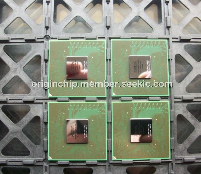
The EP2AGX45DF29C6N is a programmable logic device. The EP2AGX45DF29C6N integrates high-speed differential I/O support using the True-LVDS interface. The dedicated serializer, deserializer, and CDS circuitry in the True-LVDS interface support the LVDS, LVPECL, HyperTransport, and PCML I/O standards. Flexible-LVDS pins located in regular user I/O banks offer additional differential support, increasing the total device bandwidth. This circuitry, together with enhanced IOEs and support for numerous I/O standards, allows the EP2AGX45DF29I5N to meet high-speed interface requirements. The EP2AGX45DF29C6N also includes other high-performance features such as bidirectional dual-port RAM, CAM, general-purpose PLLs, and numerous global clocks.
Parametrics
EP2AGX45DF29C6N absolute maximum ratings: (1)Maximum gates: 1,900,000; (2)Typical gates: 600,000; (3)LEs: 16,640; (4)RAM ESBs: 104; (5)Maximum RAM bits: 425,984; (6)True-LVDS channels: 36; (7)Flexible-LVDSTM channels: 56; (8)True-LVDS PLLs: 4; (9)General-purpose PLL outputs: 8; (10)Maximum user I/O pins: 492.
Features
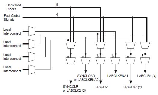
EP2AGX45DF29C6N features: (1)Programmable logic device (PLD) manufactured using a 0.15-μm alllayer copper-metal fabrication process (up to eight layers of metal); 1-gigabit per second (Gbps) True-LVDSTM, LVPECL, pseudo current mode logic (PCML), and HyperTransportTM interface; Clock-data synchronization (CDS) in True-LVDS interface to correct any fixed clock-to-data skew; Enables common networking and communications bus I/O standards such as RapidIOTM, CSIX, Utopia IV, and POS-PHY Level 4; Support for high-speed external memory interfaces, including zero bus turnaround (ZBT), quad data rate (QDR), and double data rate (DDR) static RAM (SRAM), and single data rate (SDR) and DDR synchronous dynamic RAM (SDRAM); 30% to 40% faster design performance than APEXTM 20KE devices on average; Enhanced 4,096-bit embedded system blocks (ESBs) implementing first-in first-out (FIFO) buffers, Dual-Port+ RAM (bidirectional dual-port RAM), and content-addressable memory (CAM); High-performance, low-power copper interconnect; Fast parallel byte-wide synchronous device configuration; Look-up table (LUT) logic available for register-intensive functions; (2)High-density architecture, 1,900,000 to 5,250,000 maximum system gates; Up to 67,200 logic elements (LEs); Up to 1,146,880 RAM bits that can be used without reducing available logic; (3)Low-power operation design, 1.5-V supply voltage; Copper interconnect reduces power consumption; MultiVoltTM I/O support for 1.5-V, 1.8-V, 2.5-V, and 3.3-V interfaces; ESBs offer programmable power-saving mode.
Diagrams
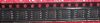
| Image | Part No | Mfg | Description |  |
Pricing (USD) |
Quantity | ||||||
|---|---|---|---|---|---|---|---|---|---|---|---|---|
 |
 EP2AGX45DF29C6N |
|
IC ARRIA II GX FPGA 45K 780FBGA |
Data Sheet |
|
|
||||||
| Image | Part No | Mfg | Description | |
Pricing (USD) |
Quantity | ||||||
|
EP2A25F672C9 |
Other |
|
Data Sheet |
Negotiable |
|
||||||
|
EP2AGX125DF25C4 |
|
IC ARRIA II GX FPGA 125K 572FBGA |
Data Sheet |
|
|
||||||
 |
EP2AGX125DF25C4N |
|
IC ARRIA II GX FPGA 125K 572FBGA |
Data Sheet |
|
|
||||||
|
EP2AGX125DF25C5 |
|
IC ARRIA II GX FPGA 125K 572FBGA |
Data Sheet |
|
|
||||||
|
EP2AGX125DF25C5N |
|
IC ARRIA II GX FPGA 125K 572FBGA |
Data Sheet |
|
|
||||||
|
EP2AGX125DF25C6 |
|
IC ARRIA II GX FPGA 125K 572FBGA |
Data Sheet |
|
|
||||||